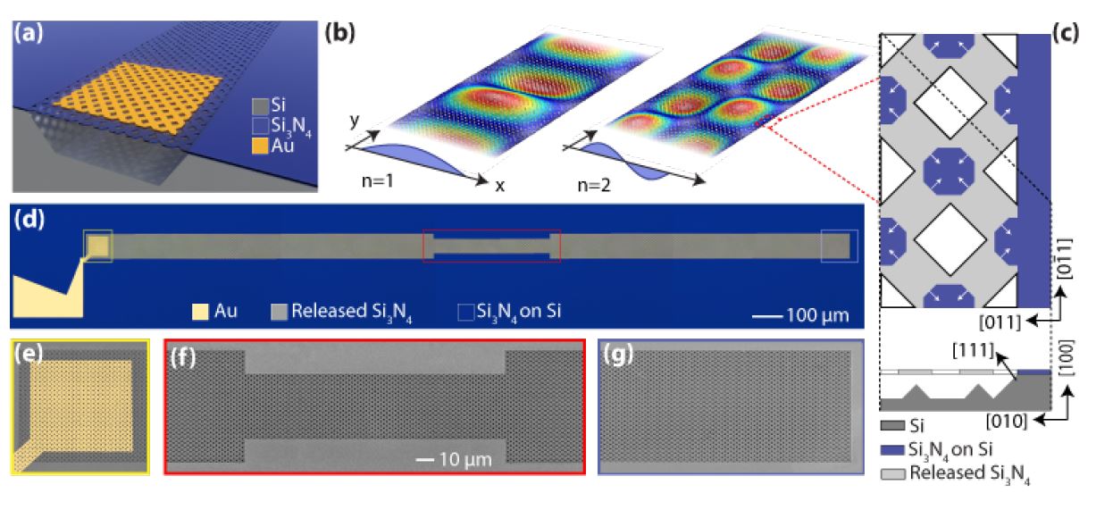
Figure 3. Meshed phononic waveguide fabrication. (a) Schematic of the meshed silicon nitride membrane released from the
silicon substrate and gold actuation electrode. (b) Finite element simulations showing the transverse mode prole of the rst
(n = 1) and second (n = 2) acoustic modes of a meshed waveguide. (c) Schematic of a snapshot of the chip during the KOH
etch. The top gure is a top-view of the chip and the mesh pattern in shown in white, the released silicon nitride is displayed
in light grey and the non-released membrane in blue. The bottom gure is a cut of the top gure along the black dashed line.
(d) Optical microscope image showing the input waveguide with a meshed gold electrode (yellow square), the tunnel barrier
(red rectangle) and the output waveguide (blue rectangle). (e)-(g) False color scanning electron micrograph of the actuation
region with a gold electrode, the tunnel barrier and the end of the output waveguide, respectively.
